These are models that are, in general, power electronics related, built in the same idealized manner. The Examples section has examples with many devices from [Pwr], so they will not be repeated here.
Quick menu:
pwr.sub:
3lvl_mod
3ph_ACMotor
3ph_br_cm, 3ph_br_vm
3ph_gen
3ph_LC
3ph_snub
3ph_SW
BrdgRect
BrdgRectThy
Cable
DC_trafo
Disturb
HystComp
Isense
RLC
SVHCC
SVPWM
UcD_block
Vsense
Wattmeter
wt
sym.sub:
sym
transforms.sub:
Transforms
Downloads

Subcircuits in pwr.sub:

3lvl_mod

Three-phase, three level modulation, with external carrier, but not restricted to 3-phase applications.
  • The inputs are internally grounded with 1GΩ, as is the external carrier control pin, EXT, and external enable pin, _EN (active low), while the outputs are , all.
  • Connecting an external carrier overrides internal settings for f, but does not disable it; set f=0 for that.
Vhigh, Vlow V Complementary output logic levels, defaults <1,0>
Vpk V Amplitude of the internal carrier, default 1
f Hz Internal carrier frequency, symmetric around zero, set to zero to disable, default 2k
a=<1m..999m> - Controls the skewness of the internal carrier (trise=a/f, tfall=(1-a)/f), default 0.5
td s Total delay time, default 1u
vh, tripdt V, s LTspice's specific for A-devices, defaults <0,0>
3lvl_mod

TOP

3ph_ACMotor

A three-phase AC motor model.
  • It has two modes of operation:
    1. Specify rotor's and stator's inductances and resistances in the SpiceLine2 line (ignore SpiceLine)
    2. For the more adventurous, set all the parameters on SpiceLine2 to zero ⇒ automatic determination of elements after the parameters on SpiceLine
    Both methods make several assumptions, such as no saturation, no air-gap losses, iron losses are not thermal dependent, etc.
  • Back EMF is modelled with current sources in parallel with 1MegΩ resistors.
  • Pins W and J output the angular speed and the torque, respectively. Loading the motor is done with a sinking current source at pin W, representing the torque (there is a schematic in Examples).
  • Inspired after The simulation of a.c. adjustable electric drive systems(Mihail-Florin Stan, Marcel Ionel, Octavian Marcel-Ionel).
  • If the .subckt line with .ic fails, .uic may be needed for simulation.
Common parameters: (needed in both methods)
Zp - Number of poles (even numbers, e.g. 2 pairs ⇒ Zp=4), default 2
J Kg*m2 Moment of inertia, default 2.1m
Direct mode: (set null for indirect mode)
Lm H Magnetizing inductance, default 351.05m
Lr H Rotor's leakage inductance, default 18.8m
Ls H Stator's leakage inductance, default 26.43m
Rf Ω Iron losses, default 2k
Rr Ω Rotor's resistance, default 5.5
Rs Ω Stator's resistance, default 7.5
Indirect mode:
Pn W Shaft's delivered power, default 1.1k
fn Hz Electrical frequency, default 50
Vn V Nominal line-to-line RMS voltage, default 400
In A Nominal current, if null, it's automatically calculated, default 2.6
eff - Efficiency, default 0.77
phi - Displacement factor (cos(φ)), default 0.78
slip - Slip factor, default 30m
DY=<0,1> - Selects the configuration:
  • 0 ⇒ delta
  • 1 ⇒ wye, default
3ph_ACMotor

TOP

3ph_br_cm, 3ph_br_vm

Three-phase switching bridges, current-mode and voltage-mode, not restricted to 3-phase applications.
  • The complementary logic inputs have internal 1GΩ pulldown.
  • There is no internal dead-time.
Ron, Roff Ω On-/off-state resistances for the switches, defaults <100m,10Meg>
Vfwd V Forward voltages for the diodes, default 0.7
Vser V Voltage drop on the switches, default 1
Rs, Cs Ω,F Series RC snubber across switches, defaults <1meg,100p>
vt V Input logic threshold, default 0.5
vh V LTspice's specific for level 1 VCSW, best keep negative, default -0.5
3ph_br_cm

TOP

3ph_gen

Three-phase voltage or current harmonics generator.
  • The outputs are marked with an arrow.
  • The internal common wye point (NUL) may be left floating if not used, depends on the schematic, but it's usually safer to add some connexion to ground.
  • The three pins at the bottom allow external frequency (FM), amplitude (AM), and phase (PM) control. All have Rin=1GΩ.
  • Anything connected to FM and AM pins overrides internal settings for f and amp.
  • The PM pin is treated differently: the general displacement is given by V(PM)+phase, where phase is either phi, for the harmonics, or phi[1:3] for each of the fundamentals.
  • The added/subtracted harmonics with h[1:3] obey the spectrum shape, e.g. if amp=1, N=0, h1=100 (default for the rest) ⇒ 100Hz@10mVpk. The phase affected by any of the h[1:3] is like in the previous point: if the value is 1 (fundamental), then phi controls the phase, else through phi[1:3] for each phase.
sym=<0,1> - Sets the symmetry between phases:
  • 0 ⇒ asymmetric, i.e. sin(nωt+φ)
  • 1 ⇒ symmetric, i.e. sin(nωt+nφ) (default)
f Hz Frequency of the fundamental, default 50
amp V Amplitude of the fundamental, default 325
phi rad Phase of the harmonics, default 0
Ro Ω Output resistance, zero means current source, default 1
N=±<0:51> - Sets the number of harmonics:
  • N>0, N=2k+1 ⇒ odd harmonics, only
  • N>0, N=2k ⇒ even harmonics, only
  • N<0 ⇒ odd+even harmonics (default -51)
  • N=0 ⇒ null output
dc1, dc2, dc3 V Per phase voltage offset, defaults <0,0,0>
A1, A2, A3 V Per phase amplitude modifier, relative to either amp or V(AM), defaults <1,1,1>
phi1, phi2, phi3 rad Per phase fundamental displacement modifier, defaults <0,0,0>
h1, h2, h3 - The values assigned to them represent a harmonic's number. When set, they will:
  • subtract the harmonic, if already present
  • add the harmonic, if not present
The indices have no meaning except to differentiate the parameters between themselves. Only their values matter. Defaults <0,0,0>
a, b, c,
d, e,
p, q,
xp, xq,
ma, mb
- Parameters for the spectrum shaper (see below), defaults <0,0,0,0,0,1,0,1,1,0,0>
tripdv, tripdt V,s LTspice's specific for B-sources, defaults <100,1u>
lim V Internal limits to avoid clipping, default 1g

The harmonics are generated based on these formulas:
x(t)=hn⋅snsin(n⋅ωn⋅t+n⋅φ)
hn = a⋅sin(b⋅ωn⋅t+nsym⋅c)+cos(d⋅ωn⋅t+nsym⋅e)
(p⋅nxp+q)xq
hn=sgn[mod(n+ma+½, mb)]

sn sets the signum on a cycle basis, where mb determines the period, and ma the offset. Setting both to zero disables the whole signum function. Non-integer values also work. The fundamental is not affected. Here are the outputs, from the 2nd harmonic up, for various settings (low means -1 and high means 1):

3ph_gen signum, click for larger view

And here are a few predefined settings to achieve some commonly found waveforms ("~" means "don't care", and "#" means the ones listed below are for ma=0, mb=0, but variations are possible for mb>1):

N a b c d e p q xp xq ma mb
Square wave
All defaults for the rest, set amp=π/4 for unity amplitude
2n+1 0 ~ ~ 0 0 1 0 1 1 # #
Reverse sawtooth
All defaults, N>0 ⇒ symmetric waveform, N<0 ⇒ asymmetric waveform. For zero starting sawtooth, set d=1/2, p=-1/2, even or odd N
±2n 0 ~ ~ 0 0 1 0 1 1 # #
UPS square wave
Variable width x=(0..0.5)
2n+1 0 ~ ~ x 0 1 0 1 1 # #
Trapezoidal
Fixed slope, variable amplitude x=[2..∞)
2n+1 0 ~ ~ 1/x -π/2 1 0 2 1 # #
Hilbert transform of a square wave 2n+1 0 ~ ~ 1/2 -π/4 1 0 1 1 # #
Alternating sinc impulses
Single (x=2), or variably-spaced double (x>2)
2n+1 0 ~ ~ 1/x -π/2 1 0 0 1 # #
Two steps square sine
x=(1..2) varies lower step's amplitude, y=(0..0.5) upper step's width
2n+1 1 2 -π/x y 0 1 0 1 1 # #
Lightning ~ 1.618 0.123 -0.321 0.333 0.258 1 0 1 1 0.618 2.718

3ph_gen

TOP

3ph_LC

Three-phase LC lowpass, delta or wye for capacitors.
  • There is no official input or output, but if used as an LC lowpass, then the image on the symbol hints at the internal configuration.
  • The null pin (bottom, internal name -1) is only active if DY=1.
L, C H, F LC lowpass, defaults <1m,1u>
DY=<0,1> - Selects between:
  • 0 ⇒ delta connection
  • 1 ⇒ wye connection, default
k=<-1..1> - Coupling factor, default 0
RLser, RLpar, RCser, RCpar Ω Parasitic series and parallel elements for L and C, all can be null, defaults <100m,100k,100m,1Meg>
3ph_LC

TOP

3ph_snub

Three-phase series RC snubber, delta or wye.
  • The null pin (bottom, internal name 4) is only active if DY=1.
R, C Ω, F Series RC snubber, defaults <100,10n>
DY=<0,1> - Selects between:
  • 0 ⇒ delta connection
  • 1 ⇒ wye connection, default
Rpar Ω LTspice's specific for capacitors, default 1meg
3ph_snub

TOP

3ph_SW

Three-phase to three-phase externally controlled timed switch, or glorified multiplexer.
  • The arrows on the symbol point towards the first channel.
  • There is an artificially generated internal dead-time, so the sum of the channels (the actual output) might show some discrepancies (dips), to avoid cross-conduction.
  • Anything connected to pin CTL overrides internal settings for ON and OFF.
Ron, Roff Ω On-/off-state resistances for the series switches, defaults <1m,1Meg>
ON, OFF s The on- and off-times for the internal timing, relative to the first channel, defaults <0.25,0.3>
tr s Rise time for the internal artificial dead-time (a lowpass RC step response), default min(ON,OFF)/1k
ref V External logic threshold, default 0.5
3ph_SW

TOP

BrdgRect

Three-phase bridge rectifier, but not restricted to 3-phase applications.
  • There are two versions: BrdgRect and BrdgRect2: the first is built with diodes + series RC snubbers, the second is built with VCSW. The second one may prove slightly faster at the cost of slightly different switching characteristics and no reverse voltage breakdown.
BrdgRect:
Vfwd, Vrev V The forward and reverse voltages for the diodes, defaults <0.7,1k>
Ron, Roff Ω On-/off-state resistances for the diodes, defaults <100m,10Meg>
Rs, Cs Ω,F Series RC snubber across the diodes, defaults <1Meg,1n>
BrdgRect2 (no reverse voltage limit):
Ron, Roff Ω On-/off-state resistances for the diodes, defaults <100m,10Meg>
lvl=<1,2> - Selects the level for the VCSW, default 2
Vfwd V Forward voltage drop across the switches, default 0.7
BrdgRect

TOP

BrdgRectThy

Three-phase thyristor rectifier with external control.
  • The _EN pin allows external enable/disable (active low), and has internal 1GΩ pulldown.
  • External firing angles are connected at the bus pin S[1:6]. The inputs are floating, and their indices indicate the order of the switches as the classical scheme↗.
  • If external firing angle control is not used, internal angle is generated based on f (frequency), phi (displacement factor), and ang (angle). phi may seem redundant, but it's there to simplify calculations for the cases where the 3-phase reference doesn't start at zero.
  • Sometimes, when external control is used, the first pulse is skipped.
  • The external control can be done with very narrow pulses.
  • Example of an externally controlled thyristor rectifier: U1, phase-modulated from -π/6..-π*7/6 by V1, generates the reference three-phase (reusing U2 might bring problems), and A1, A2, and A3 form the firing pulses. Note the order in the naming of the nets prior to transforming it in a bus for the bridge.
Ron, Roff Ω On-/off-state resistances for the VCSW, defaults <100m,10Meg>
lvl=<1,2> - Selects the level for the VCSW, default 1
Vser V The forward voltage drop across switches, should not be zero when lvl=2, default 1
f Hz The working frequency, default 50
phi rad The displacement for the base waveform, default 0
ang rad The internal firing angle, default π/5
ref V Logic threshold for external angle control, default 0.5
lim A Current limit for level 2 VCSW, default 1g
vt, vh V Threshold and hysteresis voltage for the switches, directly linked to dt, defaults <0.5,0.5> for level 1, and <0.5,0.5m> for level 2 (they are made negative internally)
dt s Dead-time, default 1u
td s Total delay for the logic, default 1u
tripdt s LTspice's specific for A-devices, default 0
BrdgRectThy

TOP

Cable

A three-phase power cable model.
  • It's a CLC Π model with terminating resistances, single cell, not as accurate for four-wire as it is for three-wire, and the three-wire may behave a bit worse than the four-wire. It's based on some formulas I found long ago, in a scan from an old book, on the Internet, which, unfortunately, I cannot find anymore.
phi m The diameter of the conductor, default 2m
f Hz Nominal frequency, default 50
len m The length of the cable, default 20
CuAl=<0,1> - Selects the conductor type:
  • 0 ⇒ copper wire (default)
  • 1 ⇒ aluminium wire
T oC The working temperature, default 27
Space m The distance between the exteriors of the insulated wires, default 5m
Dins m The diameter of the insulated wire, default 5m
TriPlan=<0,1> - Selects the geometrical formation of the wires:
  • 0 ⇒ triangular (equilateral)
  • 1 ⇒ planar
ratio=<0..0.5> - Determines the distribution of the series resistance between the terminating resistors and the cell's middle inductor. The default value of 0.5 means the resistors at the ends get half of the value, each, while the inductor has none; 0 means the inductor has all the resistance while the ending resistors have none
RparL, RparC Ω LTspice's specific Rpar for inductors and capacitors, default 100*{reactance}, each
Cable

TOP

DC_trafo

Small signal DC trafo with external duty cycle control.
  • Anything connected to the external duty cycle control overrides internal d settings.
Rout Ω Output resistance, default 1
d=<0..1> - Internal duty cycle, default 0.5
lim V Internal limits to avoid cipping, default 1g
DC_trafo

TOP

Disturb

Disturbance inducer.
  • It's a sine with offset, amplitude modulated by a modified Gaussian bell, with skewing from a tanh().
  • Output resistance is {A}Ω, and defaults to for A=0.
  • The distribution sigma is altered to mean 0.01*B at the start of the bell. In the picture below, there's ~1.05 = A + 0.01*B = 1 + 0.01*5:

    Disturb terms

A V The DC level, default 1
B V The peak of the gaussian bell, relative to A, default 0.1
delay s The delay of the gaussian bell's peak, default 0.5
sigma s The distribution, here modified to represent the time the bell reaches 0.01*B, default 0.25
xp≥0 - Multiplier for the exponent: exp(-x(2*xp)), default 1
skew<-∞..∞> - The skew factor, given by multiplication with a tanh(), default 0
f Hz The frequency of the modulated sine, default 10
phi rad The phase of the modulated sine, default 10
sq - Exponent for the time in the modulated sine, default 1
Disturb

TOP

HystComp

Hysteresis comparator with external enable and error band, and complementary outputs.
  • IN and CMP are the reference and the feedback inputs, respectively, both floating.
  • ERR allows external error control, can be dynamic, and _EN allows external enable/disable (active low). Both have internal 1GΩ pulldown.
  • The complementary logic outputs have Rout=1Ω.
  • Anything connected to ERR overrides internal settings for err.
Vhigh, Vlow V Output logic levels, defaults <1,0>
err V Internal, fixed hysteresis band (±err/2), default 0.1
dt s Dead-time, default 1u
td s Total delay time, default 1u
tripdt s LTspice's specific for A-devices, default 0
HystComp

TOP

Isense

Isolated current sensor.
G - Gain, linear, default 1
Cout F Output capacitance for aid in convergence, default 0
Isense

TOP

RLC

Universal three-phase RLC load: wye (with or without null) or delta, series or parallel, with any power combinations possible.
V V The line-to-line RMS voltage, default 400
f Hz The working frequency, default 50
DY=<0,1> - Selects the configuration:
  • 0 ⇒ delta
  • 1 ⇒ wye, default
NUL=<0,1> - If DY=0 it has no effect, else:
  • 1 ⇒ enables pin 4, default
  • 0 ⇒ disables it
SP=<0,1> - Selects between:
  • 0 ⇒ series RLC, default
  • 1 ⇒ parallel RLC
P W Active power, default 10k
QL VAr Inductive reactive power, default 5k
QC VAr Capacitive reactive power, default 2k
Rd Ω Damping resistor, only valid for directly driven reactive elements (e.g. parallel RLC). If null, it defaults to 1m
RLC

TOP

SVHCC

Space-vector hysteresis current controller, 3-phase only.
  • It's a simple approach for minimizing the number of switchings: the current stays within the inner band, if it touches the outer band, it's quickly brought back:
    O1 O2 O3 I1 I2 I3 S1 S2 S3
    1 0 0 1 0 0 1 0 0
    1 1 0 1 1 0
    x x x 0 0 0
  • Inputs marked with asterisk are the reference inputs, the others are the feedback. Both are floating.
  • The complementary logic outputs have .
Hi, Ho V The inner and outer hysteresis bands, defaults <0.1,0.2>
Vhigh, Vlow V Output logic levels, defaults <1,0>
dt s Dead-time, default 1u
td s Total delay time, default 1u
tripdt s LTspice's specific for A-devices, default 0
SVHCC

TOP

SVPWM

Space-vector PWM controller, quadrature input (sin/-cos), three-phase applications, only.
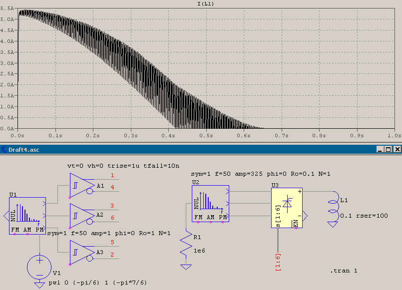
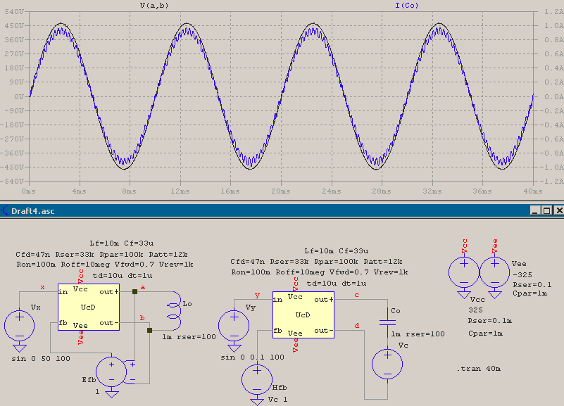
  • The inputs are floating and the complementary logic outputs have .
  • The external enable/disable pin has internal 1GΩ pulldown.
Vhigh, Vlow V Output logic levels, defaults <1,0>
f Hz Switching frequency, default 2k
sym=<1m..999m> - Controls the symmetry (skewness) of the carrier (trise=a/f, tfall=(1-a)/f), default 0.5 (symmetric)
<a,b>=<-1,1> - The signum for internal angle, atan2( sgn(a)*V(A), sgn(b)*V(b)), defaults <-1,-1>
dt s Dead-time, default 1u
td s Total delay time, default 1u
vh V Hysteresis for comparators, useful for noisy inputs, default 0
tripdt s LTspice's specific for A-devices, default 0
SVPWM

TOP

UcD_block

Full-bridge, non-inverting UcD amplifier, inspired by Bruno Putzeys↗.
  • It follows the non-inverting topology, so that the input is floating. The output is modeled with VCSW.
  • The FB pin is there to accomodate either voltage, or current feedback: bogus example. To the left there's voltage feedback, to the right it's current. The voltage mode could have used a direct connection, however given the voltage levels involved, a buffer was used.
Ron, Roff Ω On-/off-state resistances fr the VCSW and diodes, defaults <100m,10Meg>
td s Total delay time, default 150n
dt s Internal dead-time, default 50n
Vfwd, Vrev V Forward/reverse voltages for the anti-parallel diodes, defaults <0.7,1k>
Lf, Cf H, F Output LC filter, symmetric and coupled inductors, defaults <33u,680n>
Cfb, Rser, Rpar, Ratt F, Ω, Ω, Ω Feedback network, defaults <220p,1k,8k2,1k8>

Internal feedback network

vh V Input hysteresis, default 1m
RLs, RLp, RCs, RCp Ω Series and parallel parasitics for the output LC filter, defaults <1m,100k,1m,1Meg>
UcD_block

TOP

Vsense

Isolated voltage sensor.
G - Gain, linear, default 1
Cout F Output capacitance for aid in cinvergence, default 0
Vsense

TOP

Wattmeter

Wattmeter, single phase, the current flow is indicated by the arrow.
  • The pins have suggestive names: S, P, and Q are the apparent, active, and reactive powers, PF outputs the power factor, V and I output the RMS voltage and current.
  • The current sensor is a zero valued voltage source, and the voltage input is floating.
  • If there are cases where there are stalls in simulations, try loading the V and I pins with small valued capacitors. For example, if f=50, a 1µF or less should do.
f Hz The working frequency, default 50
ref V Logic threshold for the SAMPLEHOLD, ref < refidt, default 0.4
refidt V Logic threshold for the integrators, refidt > ref, default 0.5
lim V Internal limits to avoid clipping, default 1g
limsh V Limits for the internal sample & hold, variable[note]
corr - Amplification correction factor, variable[note]
[note] About limsh and corr:

SAMPLEHOLDs are A-devices, so they have vhigh and vlow as parameters, and when the output reaches those limits, the s&h doesn't simply limit the output, but cuts its amplification by a factor of 1000. This is due to the default rclamp=1, while rout=1k. This can be tested this with the following setup:

Vin in 0 pwl 0 0 1 1k ; ramp input
Vsh sh 0 1 ; 'S/H' input => acts as a repeater
Atest in 0 0 sh 0 0 out 0 SAMPLEHOLD vhigh=1 ; force upper limit to be 1

Vin feeds a ramp from 0 to 1k for 1s, Vsh forces the s&h to act as a repeater, and Atest has set vhigh=1. The output will be ~2V@1s (rout||rclamp).

On the other hand, if you want to set the limits high, it seems that 1e18 is about the limit, because at 1e19 and up glitches happen.

So, for this case in particular, if the internal limits (the squaring of powers) tend to reach 1T, or higher, a safer way to deal with the limitation is to set vhigh for the s&h to be very low, so that the 1000x attenuation is in effect early on, and simply amplify it afterwards. Precision will be affected, most likely (at these powers it shouldn't matter that much), but the limits now can be higher than 1e18, which, as high as this value already is, they can be reached when the wattemeter is used for tens or hundreds of kV and kA.

Therefore, by default, limsh==lim, unless lim>1G, when it is 1m, while the correction factor corr=1 for lim<1G, else corr=1k.

Wattmeter

TOP

wt

Angle generator.
  • The output is .
f Hz The working frequency, default 50
phi rad The initial phase, default 0
tripdt s LTspice's specific for B-sources, with fixed internal tripdv=5, default 1u
wt

TOP

Subcircuits in sym.sub:

abc-120, 120-abc

Symmetrical components analyzer.
  • There are two subcircuits contained in sym.sub: abc-120 (three-phase to symmetrical components) and 120-abc (symmetrical components to three-phase).
  • Depending on the chosen subcircuit, the pins from the sides are either inputs or outputs: abc-120 has three inputs and 6 outputs, abc-120 has 6 inputs and 3 outputs: example. The source is unbalanced with the first phase having 2 p.u. amplitude, the second a -π/6 delay, and the third a 10V offset, the only thing which cannot be recovered (V(c) compared to V(c)).
  • No matter the case, all inputs are floating, all angle outputs are , and all magnitude outputs are {-j*fmax/1n}Ω. The impedances for the magnitude outputs may seem problematic, but they were thought as monitors, only. This doesn't mean they cannot be buffered.
  • Irrespective of the subcircuit chosen, the 6 I/O pins are in pairs: magnitude above and angle below, with the order being, from top to bottom, positive, negative, and zero sequences.
  • With the exception of Cout, the parameters are all shared and common.
f Hz The working frequency, default 50
deg=<0,1> - Calculates the angles in:
  • 0 ⇒ radians
  • 1 ⇒ degrees (default)
lim V Internal limits to avoid clipping, default 1g
fmax Hz Estimated maximum bandwidth for the internal implicit hypot(), default 1Meg
ic V Initial conditions, default 0
Cout F (120-abc only) Capacitance for aid in convergence, default 1u/f
sym

TOP

Subcircuits in transforms.sub:

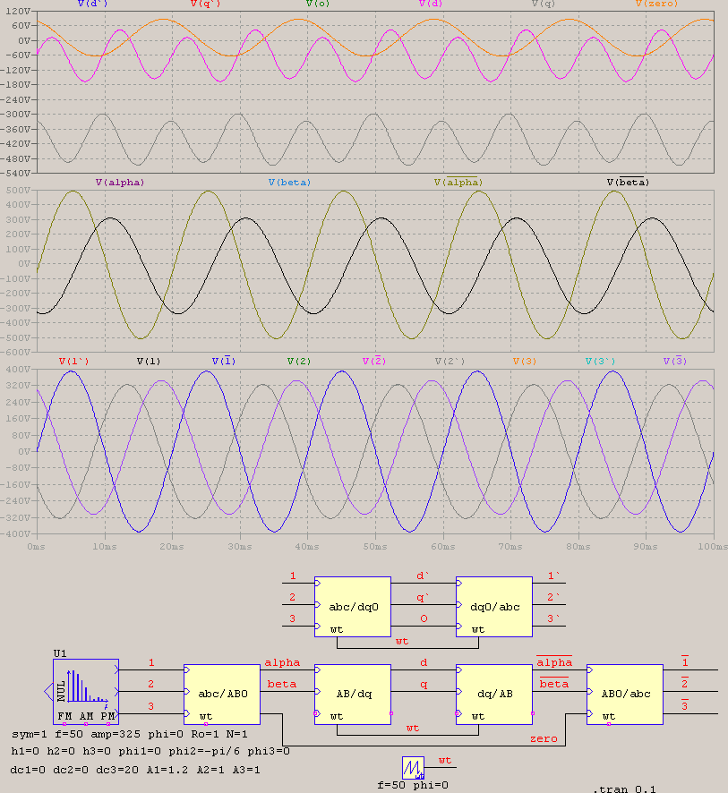
abc/AB0, AB0/abc, abc/dq0, dq0/abc, AB/dq, dq/AB, abc/120, 120/abc

Three-phase transformations: stationary frame, rotating, and symmetrical components, a quasi-instantaneous approach.
  • The subcircuit file contains: the Clarke matrix (abc/AB0) and its inverse (AB0/abc), the Park matrix (abc/dq0) and inverse (dq0/abc), and quadrature Park (AB/dq) and inverse (dq/AB).
  • The inputs are marked with squared arrows and are floating, and the outputs are . Where the matrix accepts 2 I/O pins, the third on each side, IN3 and OUT3, can be ignored.
  • The angle pin WT is only used by the Park matrices. It can be ignored in rest.
  • Example of usage: unbalanced source with phase one having 1.2 p.u. amplitude, phase two -π/6 delay, and phase three 20V offset. All voltages overlap.
sq=<0,1> - (Clarke only) Specifies whether the matrix is:
  • 0 ⇒ amplitude invariant
  • 1 ⇒ power invariant (default)
Transforms

TOP
The README file lists all the files inside the respective archive:
Pwr.zip (38987 B)
MD5=dc4d2e18b6482d8817761a9e34c7b388
SHA256=5cc8808323220497873ba001534a05fe4db4a996d1efec1c02ae9402f2a3e97d
TOP