These models are somewhat more varied, but they're included into [Filt] because they are, mostly, signal-processing related. They have the same macro-model and idealized principle behind as the others.
- Quick menu:
filt.sub:- AGC
- DeadTime
- DeadZone
- Delay
- Diff
- FreqDet
- Gain
- Integ_r
- Laplace
- LeadLag
- Lim
- LimExt
- MUX
- PhaseDet
- PID, PIDd
- PLL
- RMS
- SampledSource
- SlewRate
- SOGI
- UpDnSpl
→ filter.sub:statespace.sub:- StateSpace
- Downloads
Subcircuits in filt.sub:
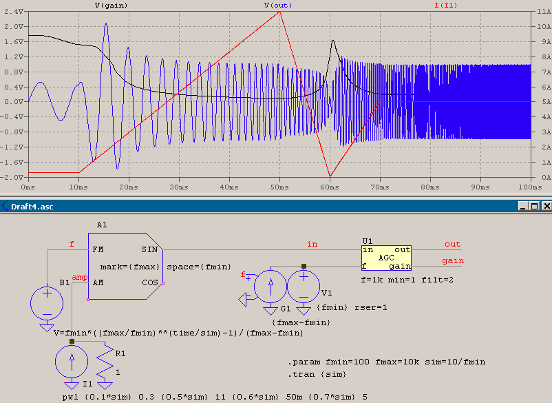
AGC
Automatic gain control, outputs the input as unity amplitude, and the gain.
|
 |
|||||||||||||||||||||
DeadTime
Dead-time.
|
|||||||||||||||||||
DeadZone
Dead-zone.
|
 |
|||||||||||||||
Delay
Delay.
|
|||||||
Diff
Differentiator.
|
 |
||||||||||||
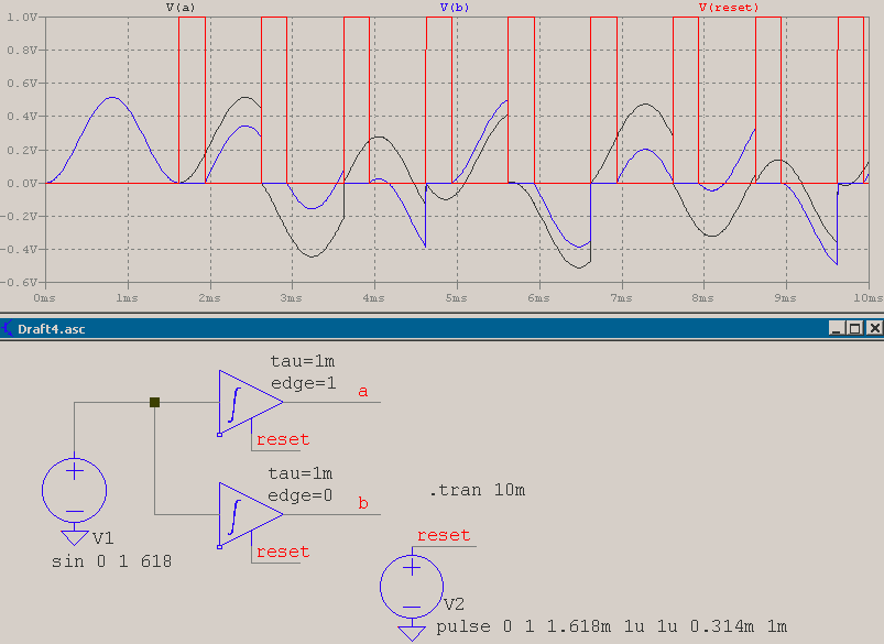
FreqDet
Frequency detector.
|
 |
||||||||||||||||||
Gain
Gain/buffer.
|
|||||||||||||||||||
Integ_r
Integrator with reset and external period control.
|
 |
|||||||||||||||||||||
Laplace
2nd order Laplace transfer function.
|
 |
|||||||||||||||||||||
LeadLag
Voltage controlled lead/lag.
|
 |
|||||||||||||||
Lim
Hard- or soft-limiter.
|
||||||||||||||||
LimExt
Hard-limiter with external limits.
|
 |
||||||||||||||||||
MUX
8-channel multiplexer.
|
 |
|||||||||
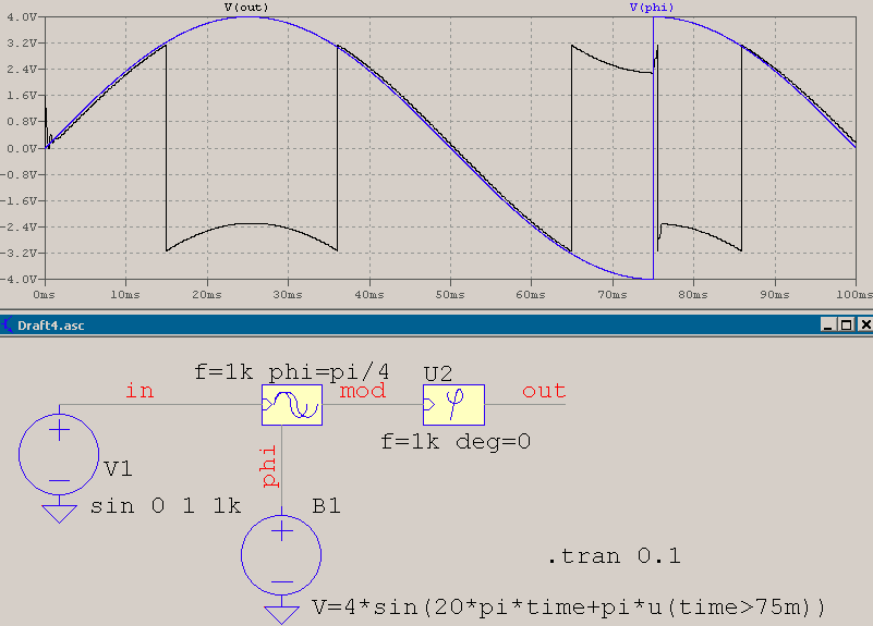
PhaseDet
Phase detector, relative to a fixed, zero displacement fundamental, starting at t=0.
|
 |
|||||||||||||||
PID
Proportional-Integral-Derivative control.
|
 |
||||||||||||||||||||||||||||||||||||
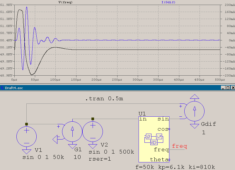
PLL
Phase locked loop.
|
 |
|||||||||||||||||||||
RMS
Root mean square detector.
|
||||||||||||||||
SampledSource
LTspice's SINE and PULSE sources, sampled.
|
 |
||||||||||||||||||||||||||||||||||||
SlewRate
Slew rate limiter.
|
 |
|||||||||||||||
SOGI
Second order generalized intergator, with external frequency control.
|
 |
|||||||||||||||
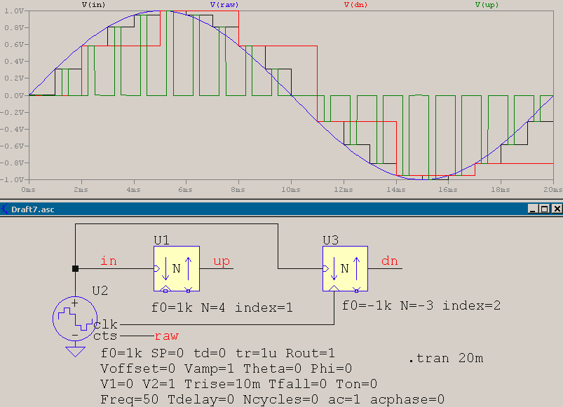
UpDnSpl
Up-/down-sampler, with or without external sync.
|
 |
||||||||||||||||||||||||
Subcircuits in statespace.sub:
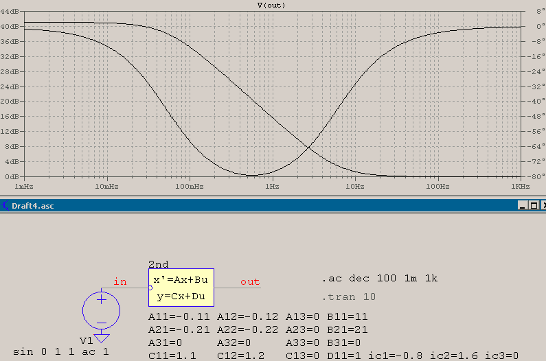
StateSpace
1st, 2nd, and 3rd order SISO state-space block.
|
 |
||||||||||||||||||||||||||||||||||||||||||
The README file lists all the files inside the respective archive (including Filter.asy and filter.sub):
- Filt.zip (77368 B)
- MD5=f05deb9f5e17f2e3021136434403bf1b
- SHA256=e22256aa2fd6390b752889aeb54bd9fbb5b28d6d02a7fcff684925792cabd4dd